Introduction
Printed Circuit Boards (PCBs) are essential in contemporary electronics as they serve as the base that connects and organizes electronic components in different devices like smartphones, computers, industrial machinery, and aerospace systems. In this detailed article, we will explore the world of PCBs, looking at their creation, types, design considerations, manufacturing techniques, and applications in various industries.
Understanding Printed Circuit Boards (PCB)
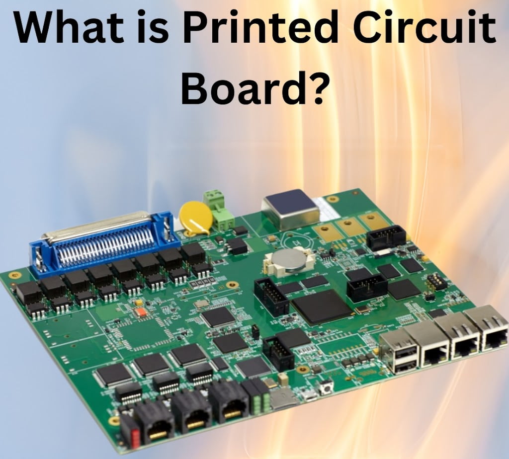
A Printed Circuit Board (PCB), made from non-conductive substrate material like fiberglass or composite epoxy, consists of conductive pathways etched or printed on a flat board. Copper conductive pathways are used to form the electrical connections among components such as resistors, capacitors, integrated circuits (ICs), and connectors on the PCB.
Components of a PCB
Substrate Material
The main material of the PCB, one that supplies the mechanical support and insulation. Traditionally, the substrate materials used to be fiberglass (FR-4), ceramic, and flexible materials such as polyimide in the case of flexible PCB.
Conductive Traces
Copper is used to form thin tracks on PCBs that are the electrical circuits that link the different components and transfer the electrical signals.
Pads and Vias
Pads are PCB surface areas where electronic components are soldered or mounted, whereas vias conduct the connection between different layers of the PCB and made of plated holes.
Silk screen
The silk screen layer has parts such as markings, labels and element’s prints that help the manufacturing, testing and the identification of the components.
Solder Mask
A protective coating is made to reduce short-circuit and corrosion risks when soldering the copper interface lines and pads.
Kinds of Printed Circuit Board (PCB)
PCB come in various types and configurations to suit different applications and design requirements:
Single-Sided PCB
On one side of them, there are copper prints, and they are often employed in basic electronics, with the quantity of components being fewer.
Double-Sided PCB
Copper through-hole connections can be observed on both sides of the board communicating via vias. Multilayer Class of PCB implement doublesided structure, which provides more routing flexibility and suited for multiple, complex circuit configuration.
Multi-Layer PCB
Layer of substrate is the base for printed circuit boards and the conductive traces are manufactured between the bases. They allow higher component densities, reduced size and improved signal quality so they are perfect for electronics that are smartphones, computers and other similar advanced electronics.
Rigid, Flexible, and Rigid-Flex PCB
The Rigid PCB is known to have fixed geometry, the Flexible PCB can be bent and conforms into curved surfaces, while rigid-flex PCB includes both rigid as well as flexible parts that provides an opportunity in designing and packaging.
Design Considerations for PCB
Designing a PCB involves several key considerations to ensure optimal performance, reliability, and manufacturability:
- Component Placement:Provide a plan of components in such a manner to avoid signal interruption,amplify the strongest signal and facilitate a quicker assembly and testing.
- Trace Routing: One of the key RF design and routing challenges in printed circuit boards, especially in high-speed digital and RF applications, is to carefully set up traces to preserve signal integrity, eliminate cross-talk, and follow the impedance requirements.
- Power and Ground Planes: The development of unified power bus and reference plane to offer uniform voltage distribution, reduce noise, and enhance EMC (Electromagnetic Compatibility) performance.
- Thermal Management: Ensuring effectiveness in heat dissipation through thermal vias, heat sinks, and devoted component placement to mitigate the risk of overheating and be able to endure long-term reliability.
Production of the PCB
The manufacturing of PCB involves several steps, including:
- Design and Layout: Embellishing the workflow with the PCB design software, building the schematic, laying out the traces, and routing, minding the element of the distortion of signal, components placement, and thermal management.
- Prototyping: Iterative production of a prototype printed circuit board with a few rapid prototyping techniques like CNC milling or 3D printing approaching the required optimized design.
- PCB Fabrication: These involve practices like etching that consists of the removal of unwanted copper to form the tracing, and drilling which is used to form holes for components mounting and vias.
- Component Assembly: For the PCB assembly SMT (Surface Mount Technology) or through-hole assembly techniques are adopted to solder components on the PCB followed by checking and the quality check to ensure the functioning.
- Final Testing and Quality Control: PCB are subjected to stringent testing measures such as electrical testing, testing of functionality, and of inspection for errors in order to match the desired performance levels and reliability standards.
Applications of PCB
PCBs are integral to a wide range of industries and applications, including:
- Consumer Electronics: Use of PCB in smartphones, laptops, TVs and appliances at home provide that electrical connectivity which is required by modern devices.
- Automotive Electronics: In cars, they govern functions such as engine management, infotainment systems, safety systems and EV components.
- Industrial Automation: The PCB are indispensable components in control systems devices, PLC (Programmable Logic Controllers), robotic process automation and sensor interfacing used in industrial machinery and automation.
- Aerospace and Defense: The PCB are employed in avionics systems, radar, satellites, communication equipment, and military electronics, where performance and reliability are very critical.
- Medical Devices: PCB are essential to medical imaging, various monitoring devices, implantable devices, and diagnostic instruments which contribute to the innovations in healthcare technologies.
The future of PCB technology is marked by several trends and innovations
- Miniaturization: Further miniaturization of components and PCB to follow the trend of smaller and more convenient digital items.
- High-Frequency and RF PCB: The proliferation of high frequency and RF PCB in various applications such as, wireless communication, Internet of Things (IoT) devices, and 5G network infrastructures.
- Advanced Materials: Utilizing new-generation materials, such as flexible substrates, high-temperature laminates, and conductive inks for the sake of performance and reliability.
- Embedded Components: Integration of passive and active components right into the PCB substrate for the size reduction, enhanced signal quality and minimized assembly.
Conclusion
To sum up, Printed Circuit Boards (PCBs) are essential parts that support the operation and connection of contemporary electronics in various sectors. With the continued advancement of technology, the processes for designing and manufacturing PCBs will progress in order to cater to the requirements of more compact, quicker, and more effective electronic systems, leading to innovation and influencing the future of electronics.